What if you want to make a PCB, like, right now and not wait for a PCB fab to make them and send them to you? Or, what if you want other stuff etched into a copper layer that would be hard to pack into the Gerber files that board houses want? Well, if you have an MSLA resin printer, honestly, you’ve already got a pretty much perfect tool for the job. We’re going to try a quick and dirty method today, that is, one of the ways is quick, the other is dirty, and only one of them works, but it does work incredibly well.
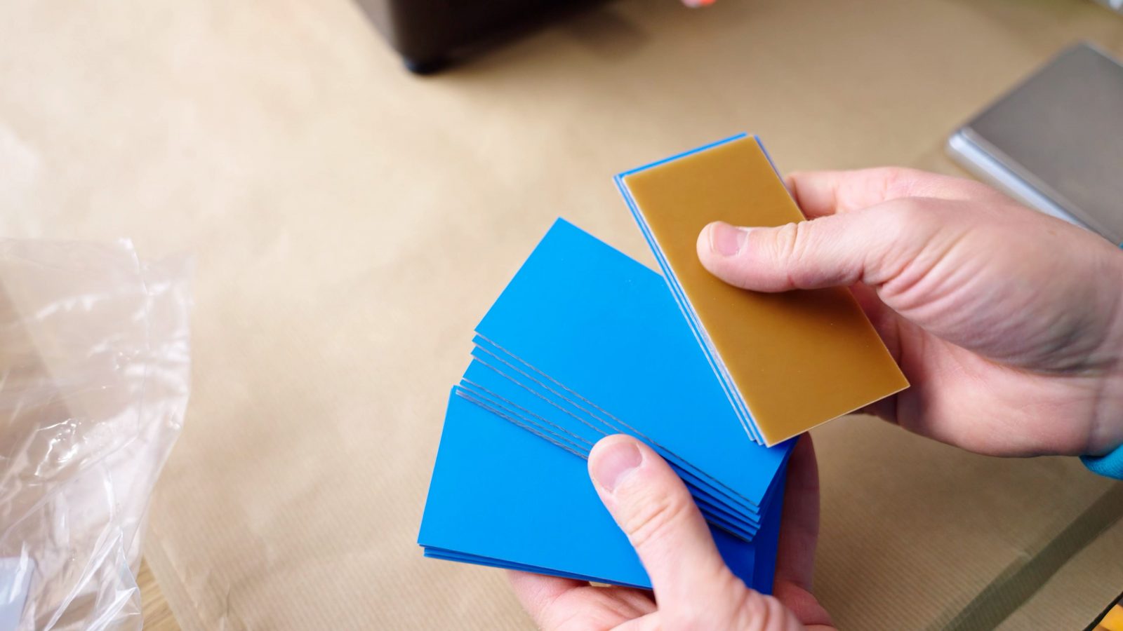
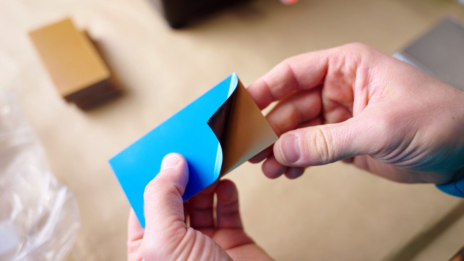
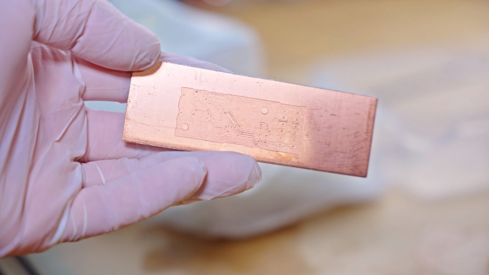
So basically the standard way of making PCBs is by using photosensitive coated stock material – like this. It’s a pretty simple buildup. You’ve got your carrier material on the bottom, this is glass fiber or paper typically, then you’ve got a full sheet of copper, and with the photosensitive ones, you also get a thin coating that reacts to UV light.
This thing also uses UV light to cure layers, you see how this is coming together?
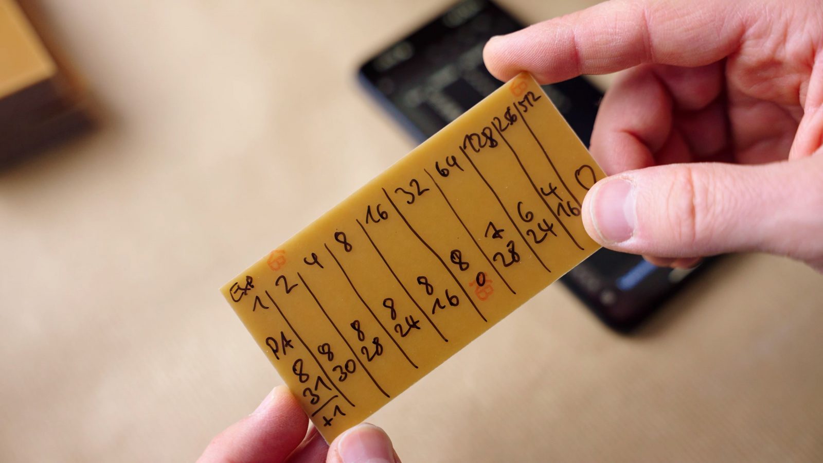
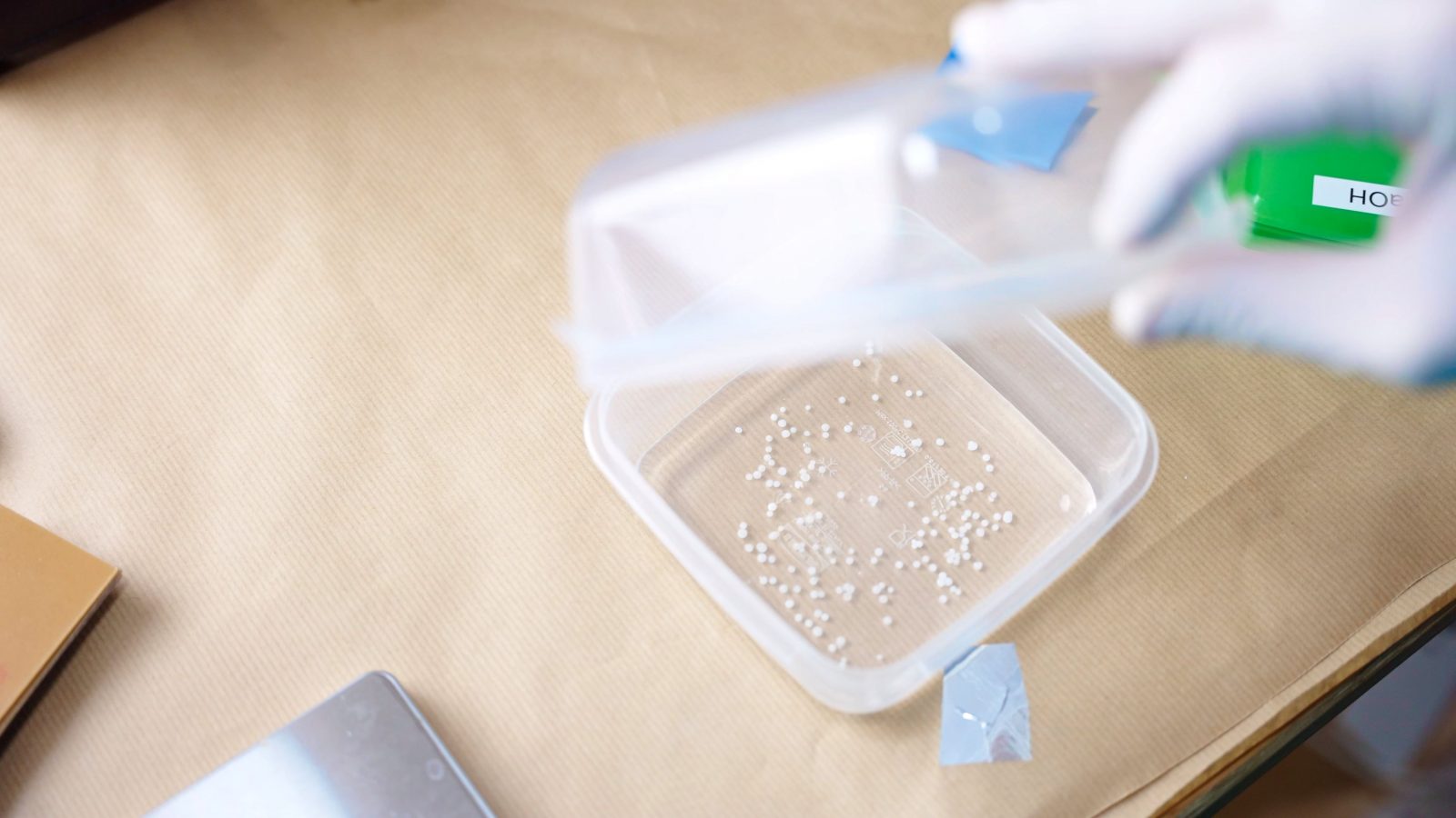
The first thing we need to do is to figure out how long we should be exposing the photo film on this. What you find online is anywhere from a couple of seconds up to 10 minutes of exposure time, depending on which UV light source you use. So I laid out an exponential time scale, starting with 1 second, 2 seconds, 4 seconds, and so on, up to a bit over 8 minutes, so that allows me to cover a huge range of possible exposure times in one go. The raw PCB gets taped down and then, at set intervals, I can pull out this piece of paper that I covered with aluminum tape to make it completely opaque.
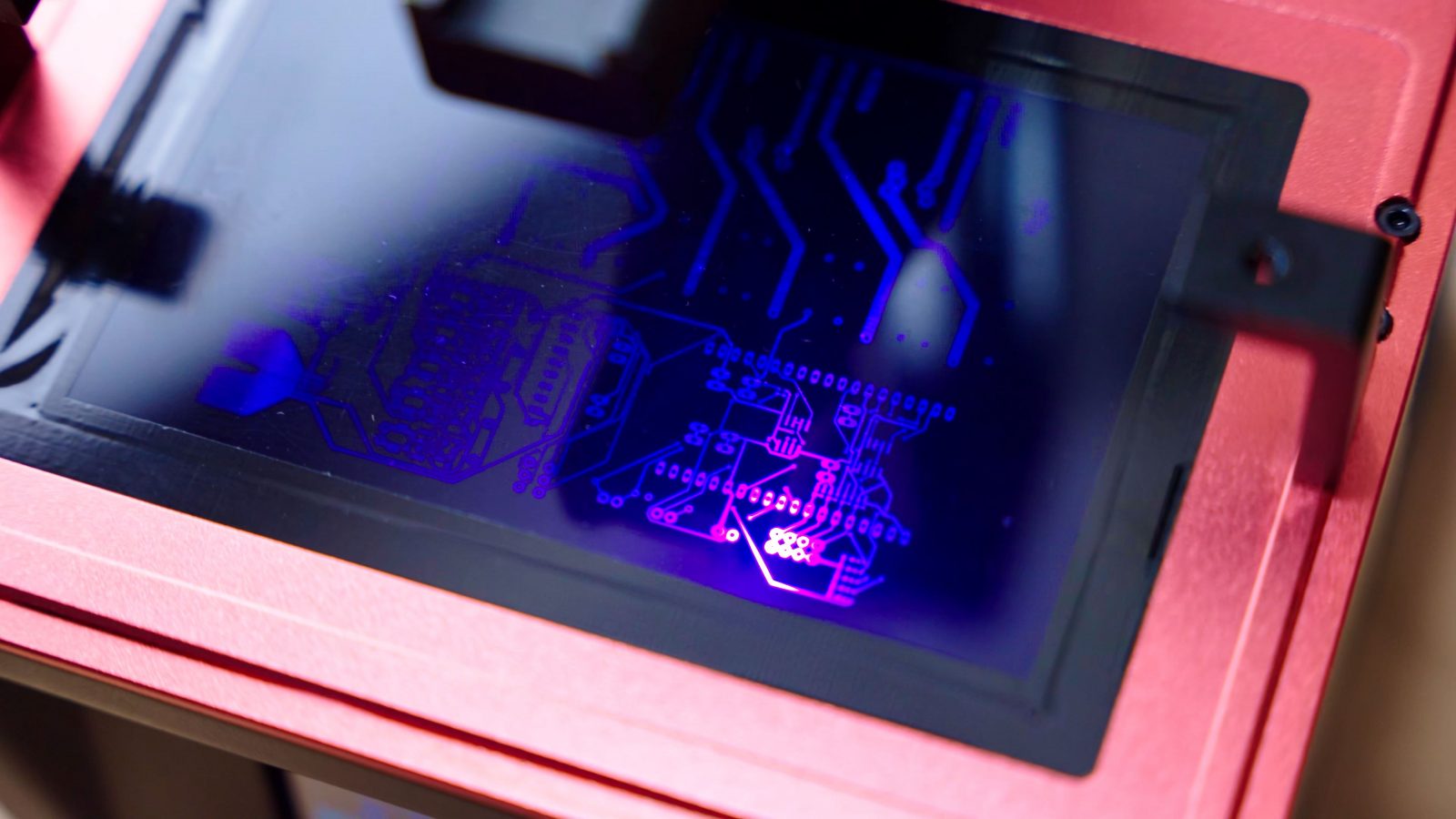
Typically, you print your PCB layout onto a mask that sits between the UV light source and the coated PCB. But the “M” in “MSLA” printer already stands for “mask”, so here we can just use the printer’s LCD for that. I’ve got the PCB layout loaded up and I’ve set the exposure time to 10 minutes total, which should be enough to run this trial.
At this point, you can’t really see that anything would have changed, and that’s because we still need to develop the photoresist layer.
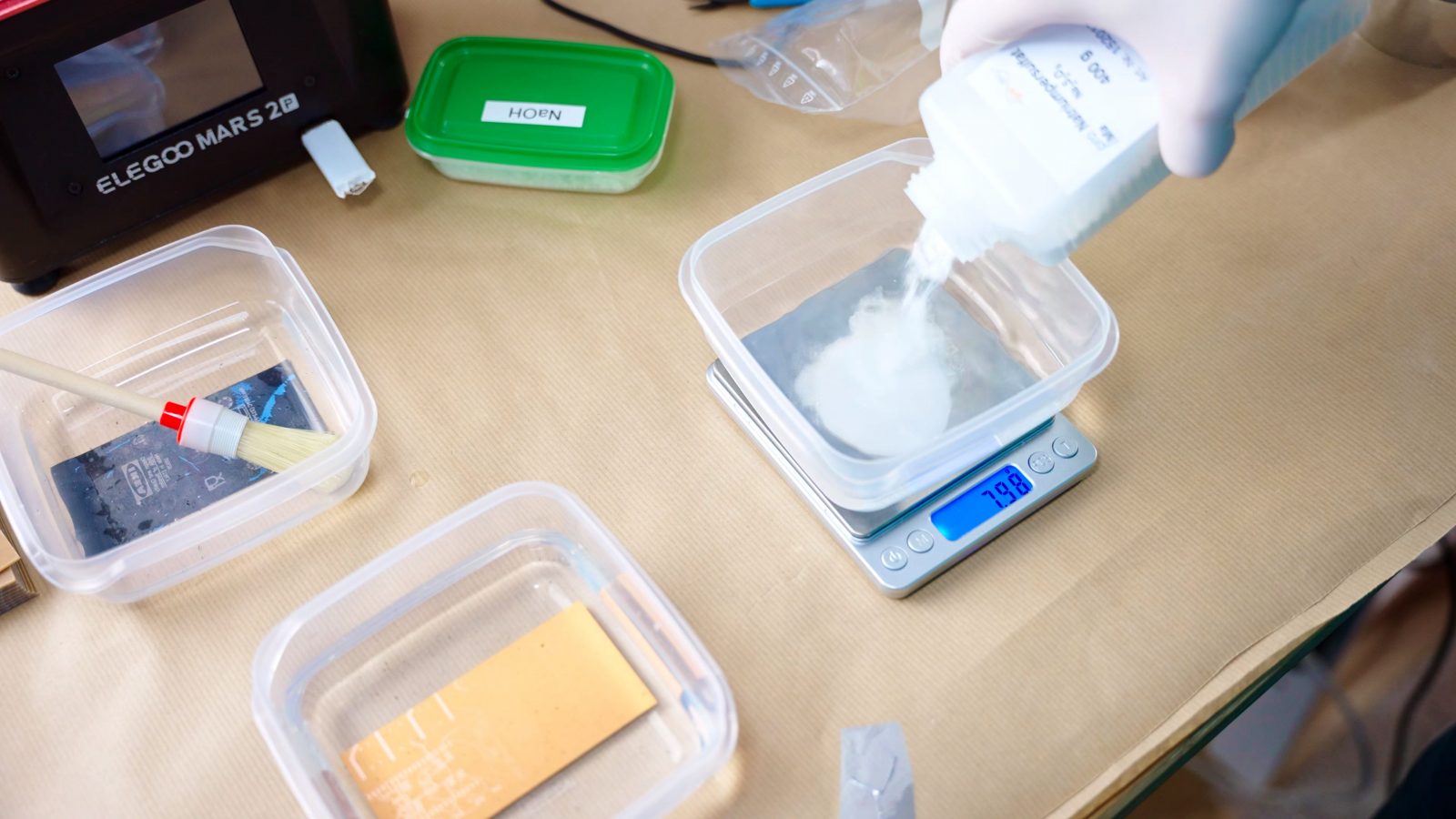
So, quick note on the chemicals used here. To develop the photoresist, what you use is a solution of sodium hydroxide in water, aka lye or caustic soda. This stuff is not to be messed with. Sure, it’s a great cleaning product for household use, but it’s also really great at cleaning the skin right off of your flesh or cleaning out your eyesight if you get some in your eye. So I’m always wearing latex gloves in this case, they’re a bit more resistant than the nitrile ones you’d use for resin, I’m also wearing an extra layer of goggles and I’ve got a bottle of vinegar on hand if some of it does get on my skin, so I can immediately neutralize it.
Then, to etch the copper I’m using sodium persulfate, which also isn’t exactly healthy, it’s a strong oxidizer, so use it with caution. And maybe use proper lab-grade containers to work in and not the Ikea containers I happened to have at hand.
So with that out of the way, in we go!
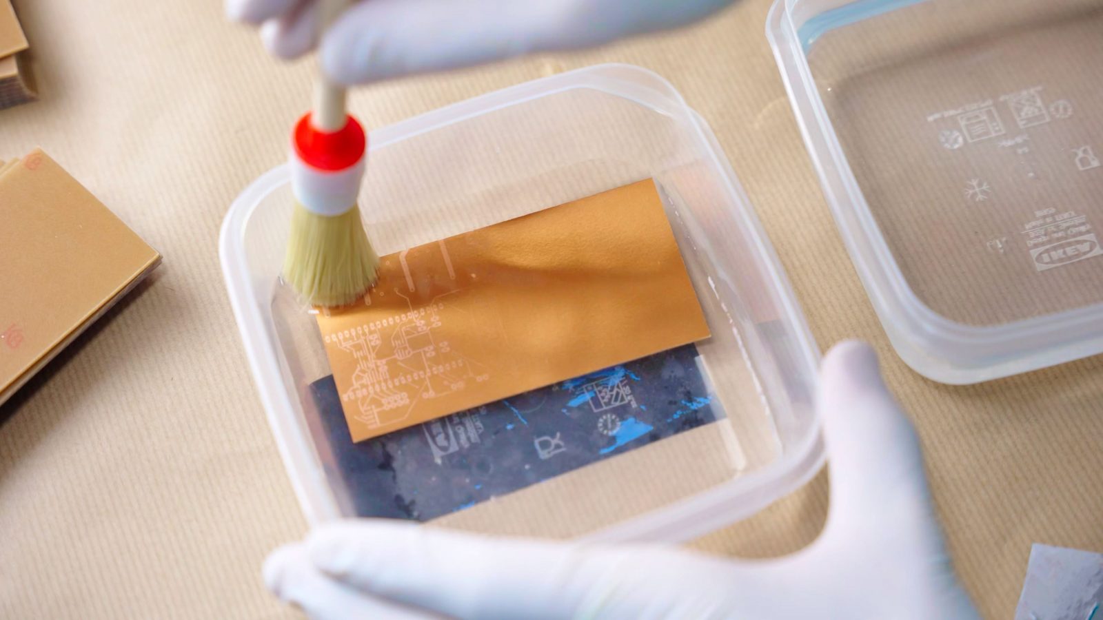
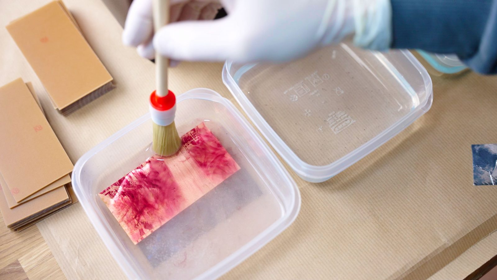
You can immediately see that red wash that’s coming off of the board – I’m helping it along a bit with a soft brush, and after a couple of minutes, it looks like the exposure is mostly done. You can really see where there’s photoresist left and where it’s been taken off.
Typically, you would need to do all of this in a dark room to avoid exposing the rest of the board, but since I am in a dark basement room and the only light in here is an artificial LED light that has no UV components, I can work with it a bit more easily.
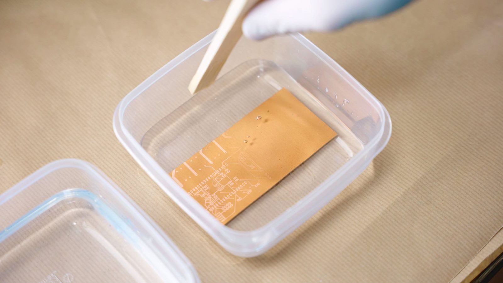
Last step, in for the etching, and we’re done!
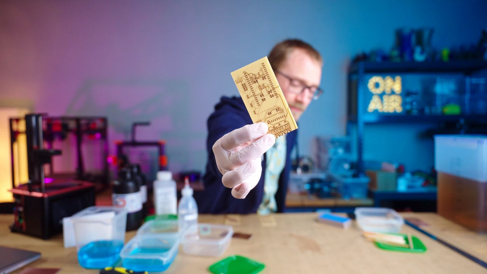
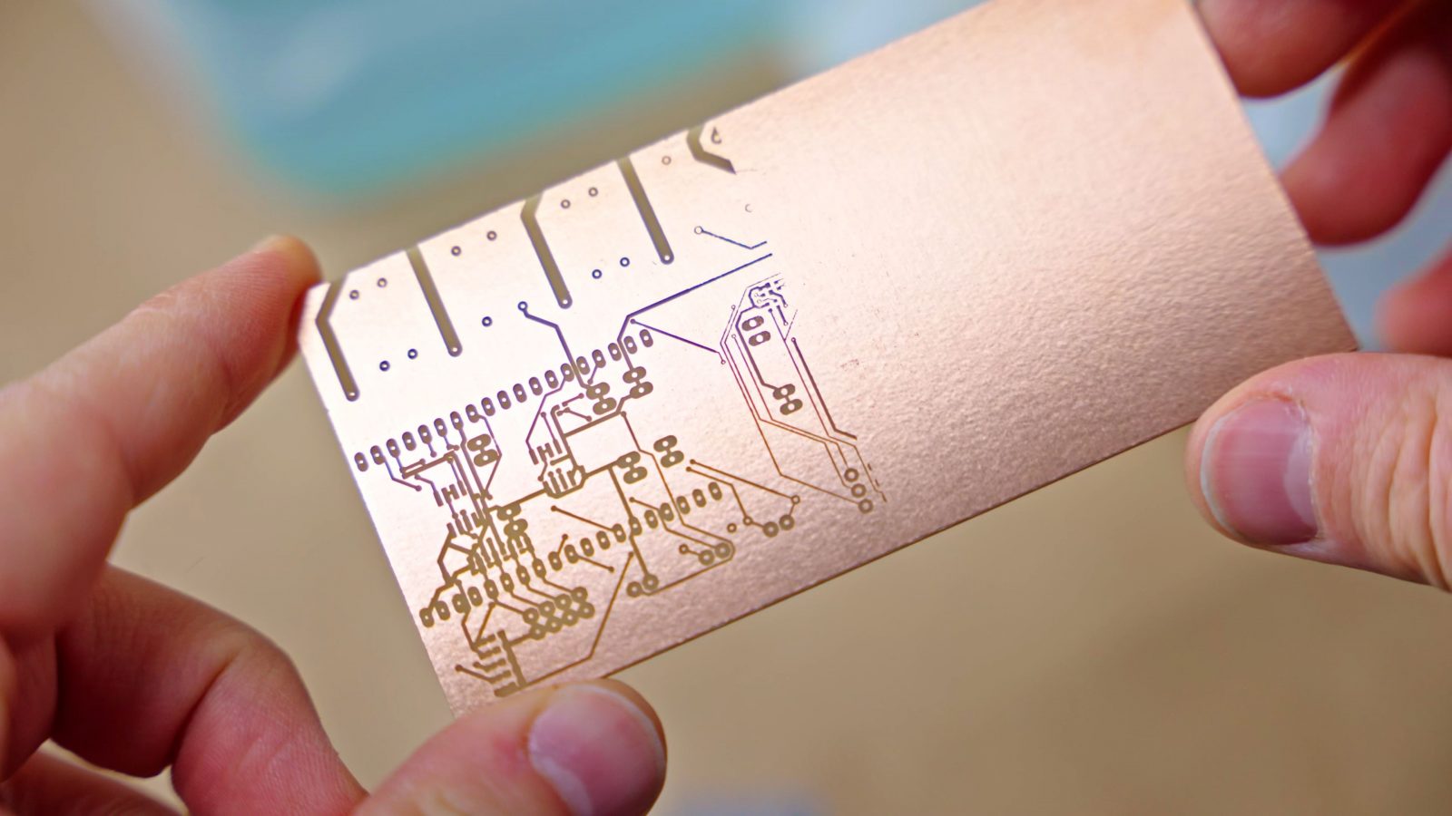
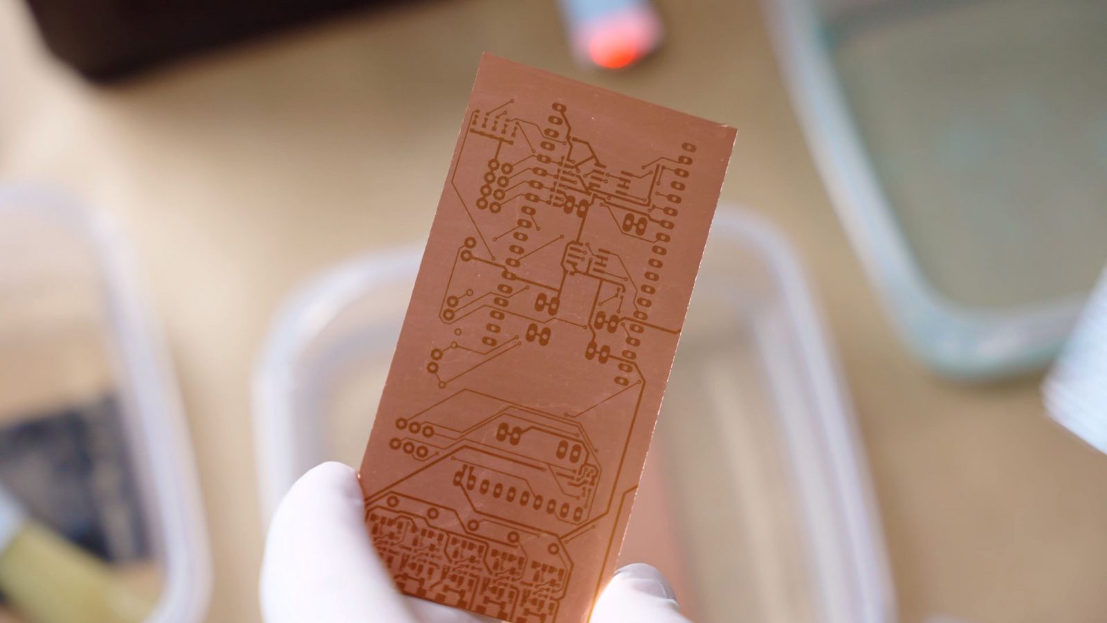
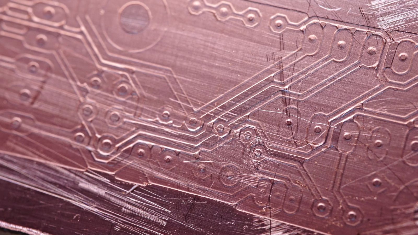
So here is that first PCB that we made, and honestly, it did turn out rather nicely. So you can see that all the structures are nicely there, there is no sign of pixels from the printer’s LCD and about 6o seconds, so one minute seems to be the right amount of exposure for the Elegoo Mars 2 Pro. 32 seconds seemed to have a bit of trouble getting all the photoresist off and properly exposing it, but once you go beyond 60 seconds, we’re actually getting overexposed and we’re removing more of the photoresist than we have to. So 64 seconds seems to be pretty good.
Now, the only problem with this is that we made a negative of the actual PCB!
These are called “photopositive” PCBs but I guess that applies to the areas that you apply light to then actually dissolve once you put them into the development solution. So what we’re going to have to do is to invert the files that we’re feeding the printer and I’m going to show you how that process works right now.
For this process, I’m using Eagle and Fusion 360. I know I probably should be using KiCAD and FreeCAD, but this combo works pretty well for me.
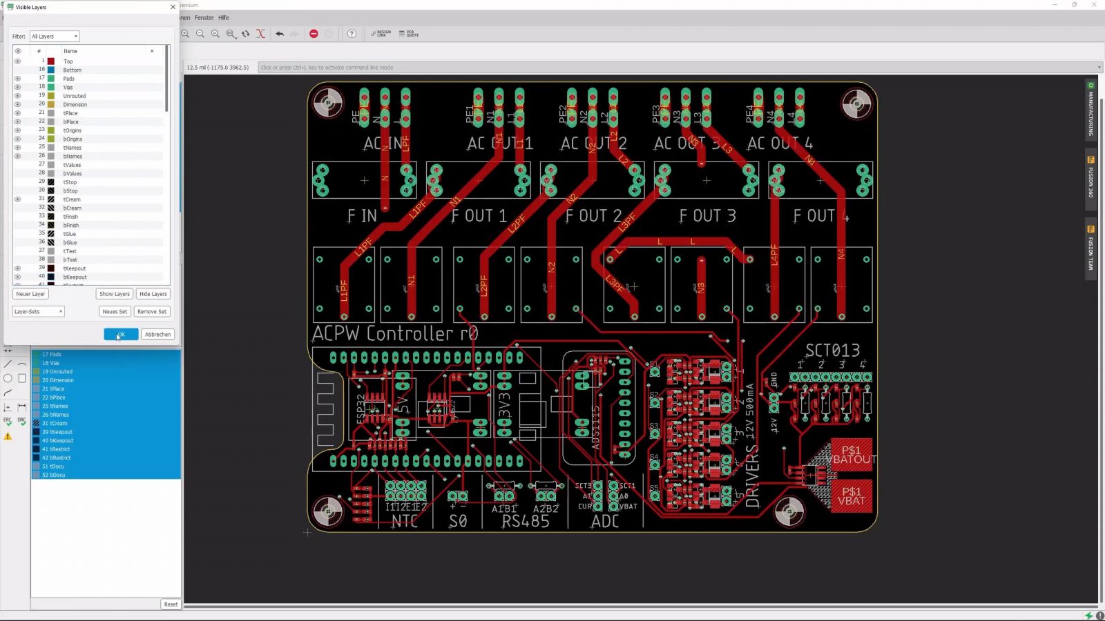
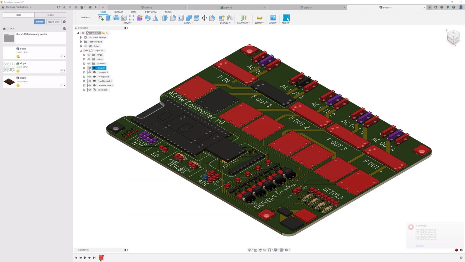
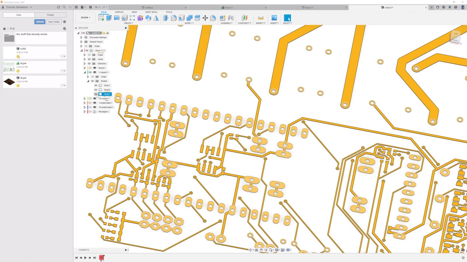
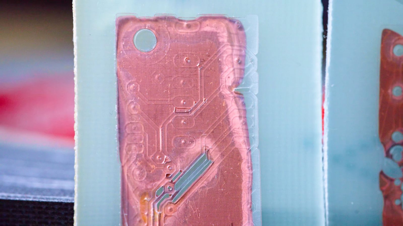
Basically, I created my PCBs as usual in Eagle, saved them, and then directly opened the Eagle files in Fusion. There, you can swap over to the “3D PCB” view, save that as a new Fusion file, then create another empty file in Fusion drag in the 3D PCB file, break the link and you’re good to go! There will be a couple of different “copper” bodies inside the part, one is traces and pads, one is fills and one is an extra layer for just the pads. Since, for these boards, we need a negative model of the traces, I’m drawing a quick box around all the traces and I’m then subtracting all the traces I want from that block. Then I can just export what’s left as a mesh and import it into the slicer, in this case, Chitubox.
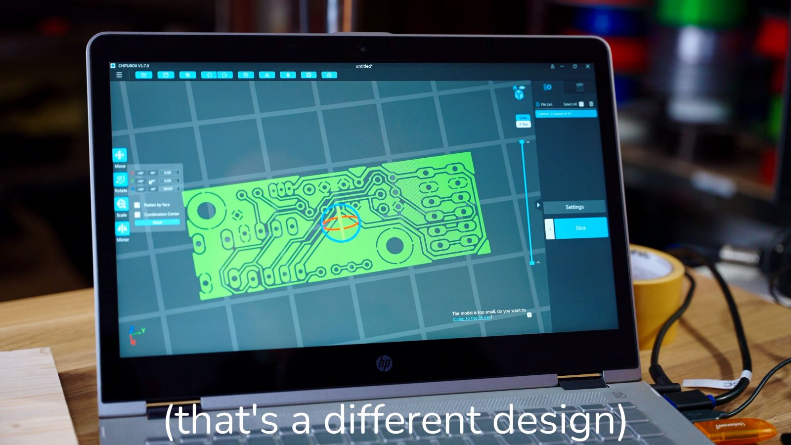
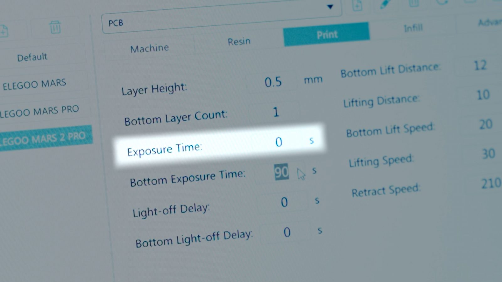
Make sure the orientation is correct – the design needs to be flipped – and then increase the exposure time for the first layer up to the value we got from the exposure test earlier. I’m also setting exposure times for the other layers to 0 just to be safe. Check the preview, export, and you should be ready to expose some PCBs!
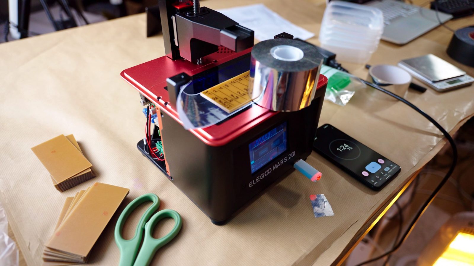
Of course, this process could probably be easier, but since the Mars 2 Pro that I’m using as my main experimentation platform is using the whole Chitu ecosystem, you’re kinda bound to their tools.
Okay, rinse and repeat, and whoops! That’s what happens when you add 14g of sodium hydroxide instead of 1.4g. Yeah, that’s a little too well-developed.
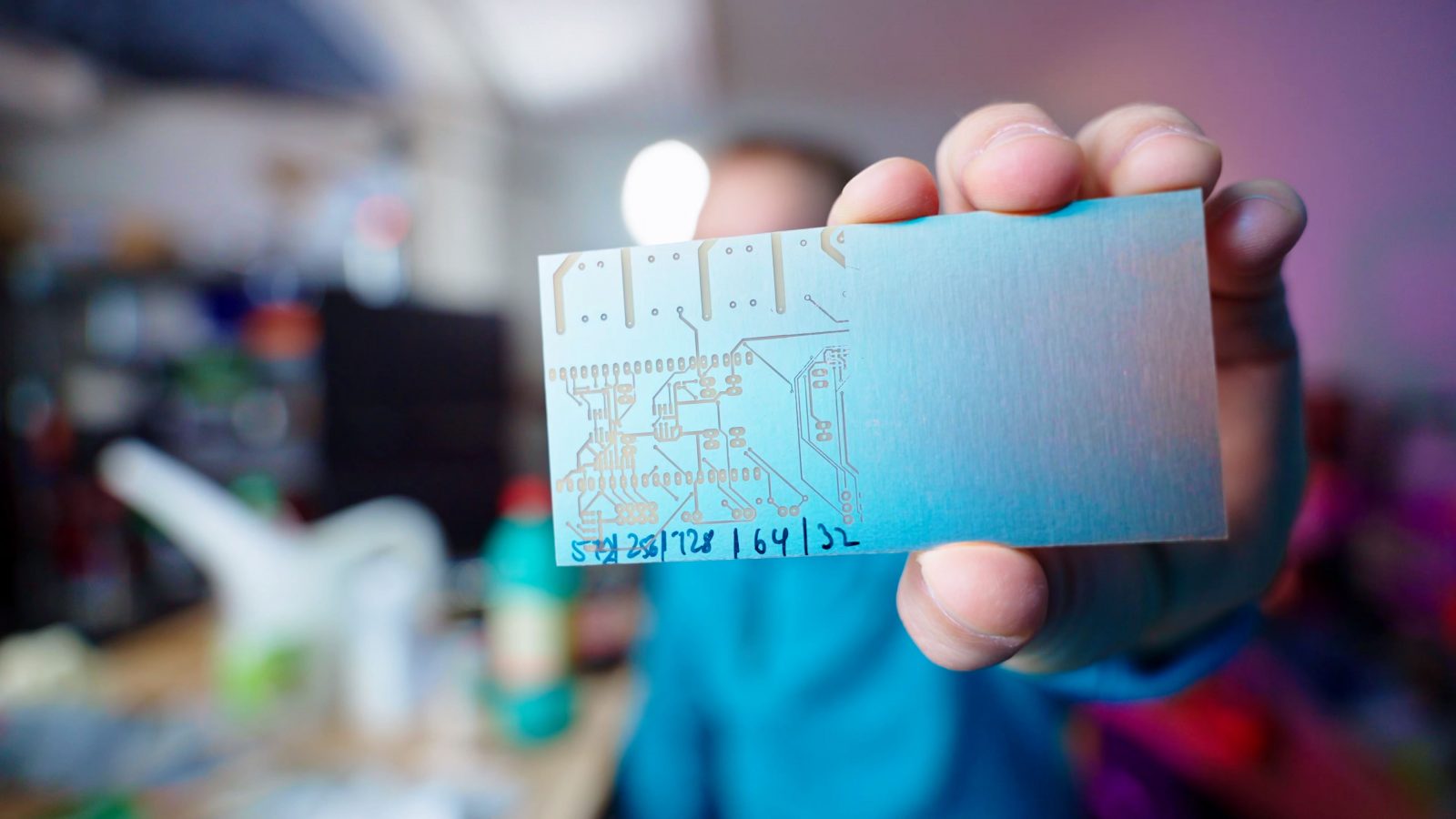
The PCB with 60 seconds exposure came out okay, so I did a second one with 90 seconds, and that one looks pretty much perfect.
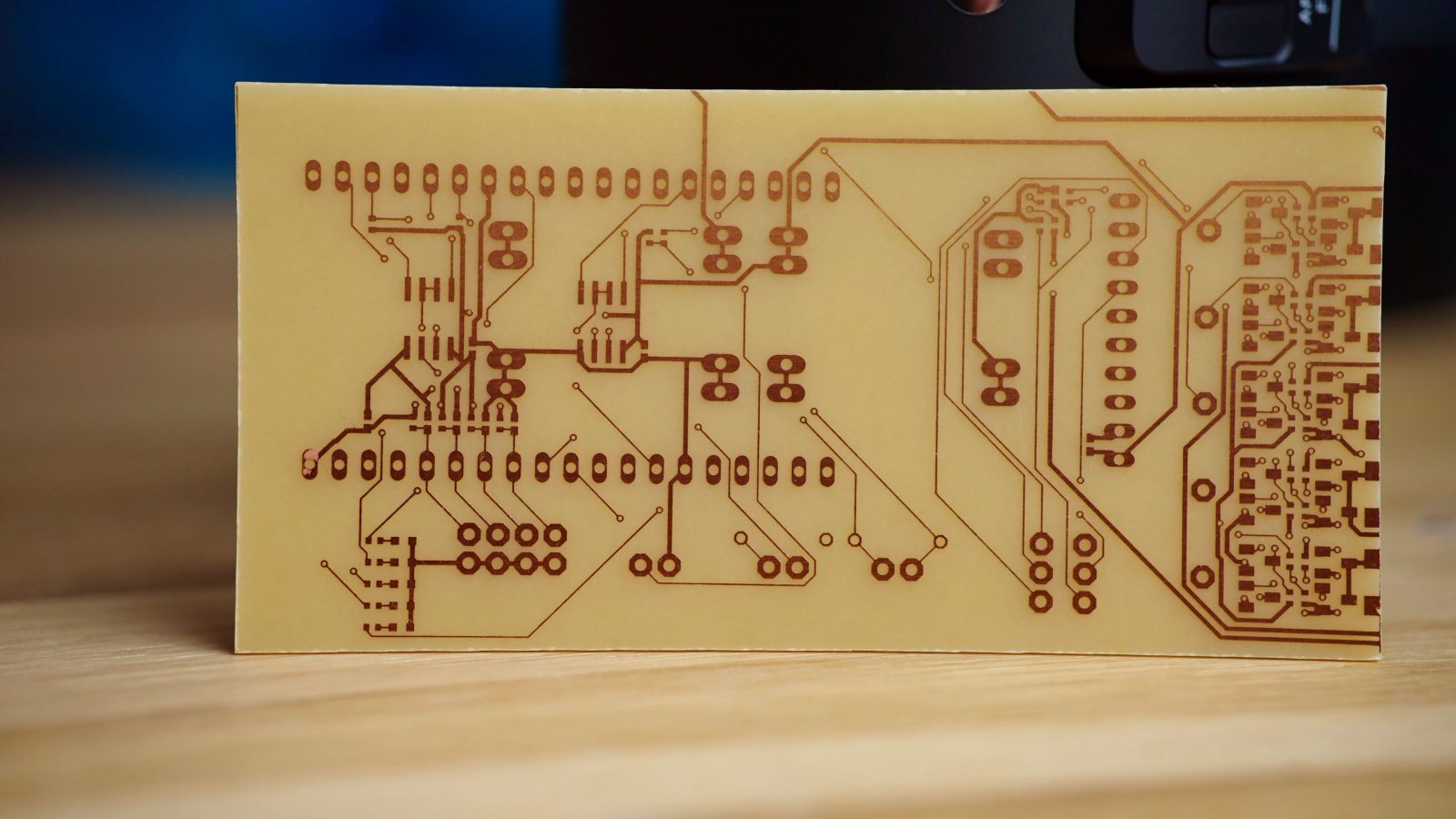
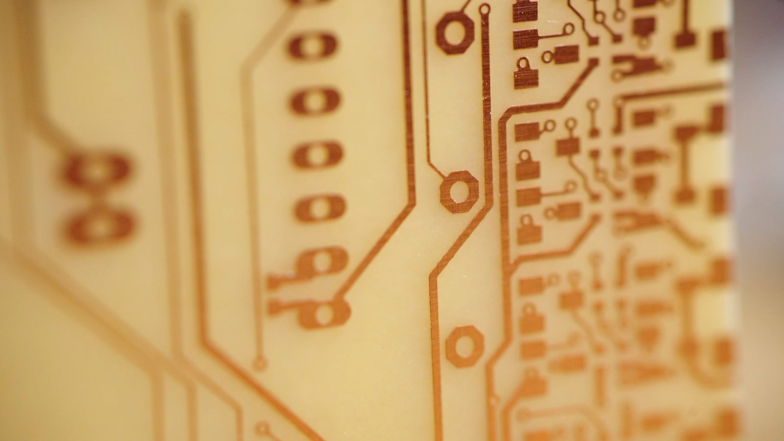
I’m really happy with how this turned out! This is a perfectly usable PCB, you get really crisp details, the fine traces look great, for through-hole parts, the only thing you’ll need to do is to drill the holes, but that’s a fairly quick process. I mean, making PCBs at home is not something you want to do in bulk, but it’s more for reducing the cycle time between having an idea, making and trying a PCB, and then making the next revision on it right away.
So the other thing I tried was using a blank copper-clad board without the photoresist. These are FR4 boards, and you can cut them by deeply scoring them with a knife and then snapping them off.

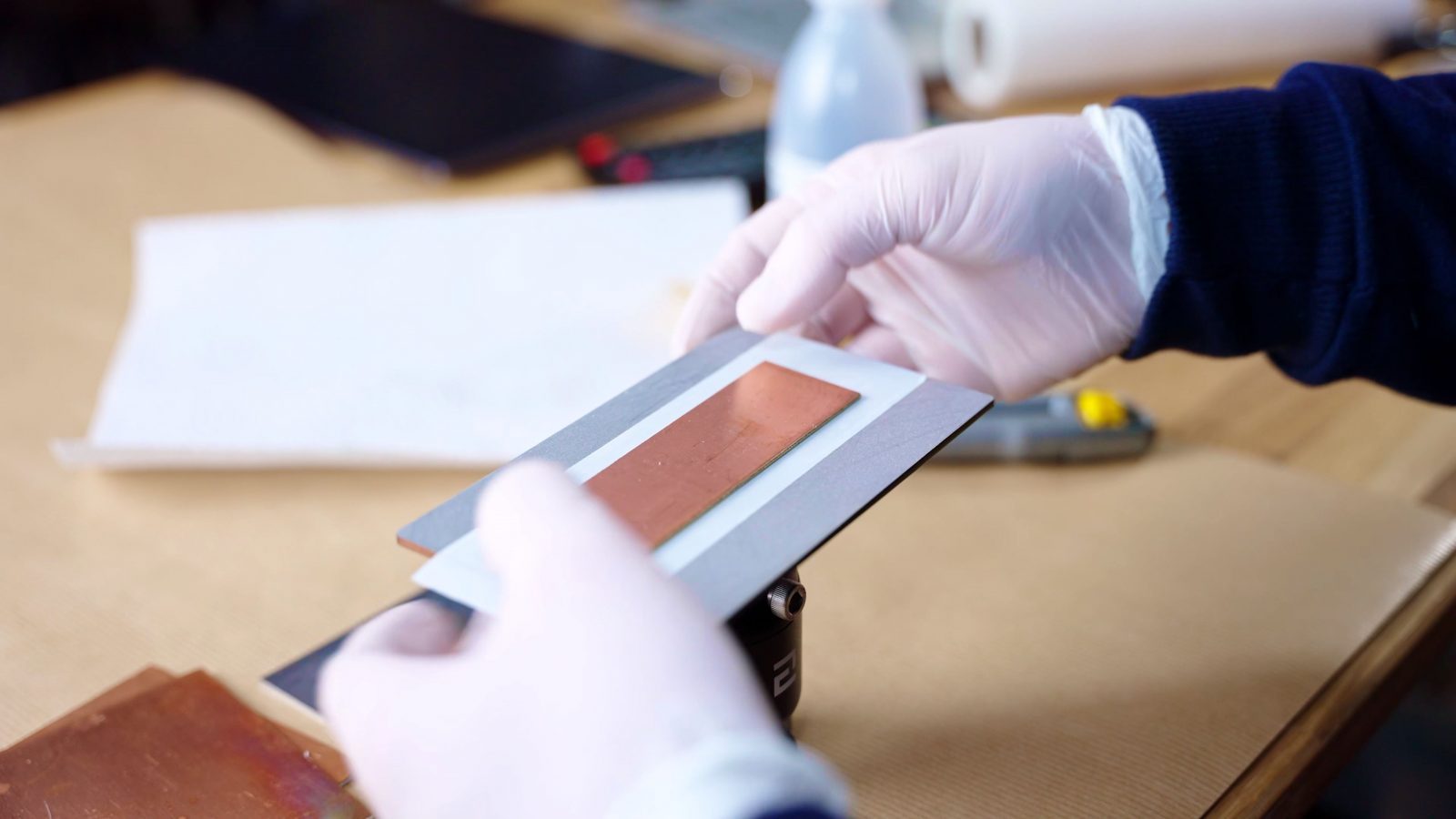
Don’t saw these when you don’t have to, the dust is nasty. So, double-sided tape onto the bottom of the print platform, which I releveled, of course, added some resin, I’m using the clear version of Siraya “Blu” resin, and then I simply cured some resin onto the copper. And surprisingly, the resin sticks really well to the bare copper. You can even make out the finer traces already after washing.
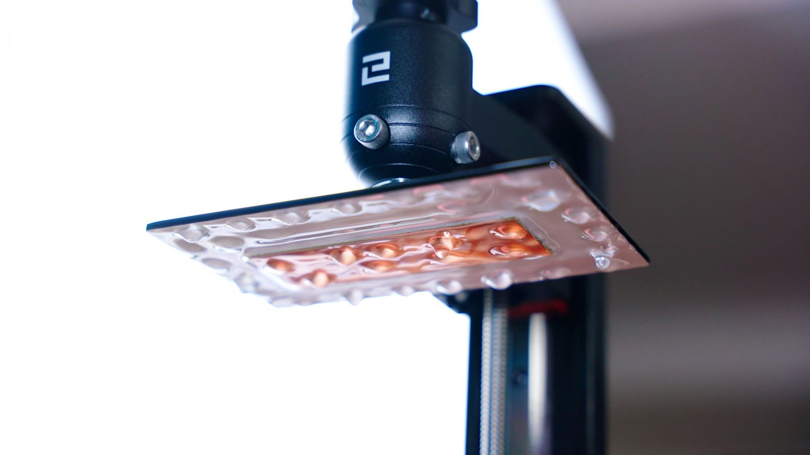
The only problem with it here is that it seems impossible to find a balance between undercuring the first layer and not having it stick well and overcuring it and covering up the channels that should remain open so that we can etch out the insulation channels. Unfortunately, even leaving the board in the etching solution overnight, they only got etched around the corners and on larger gaps, but you don’t see anything of the actual traces.
Maybe one cool application of curing resin onto a PCB is adding your own solder mask and silkscreen over the bare traces. I was considering trying Siraya Tech’s high-temp sculpt resin for that, but a) it didn’t get here in time and b) I don’t know what sort of fumes that will give off when you solder against it.
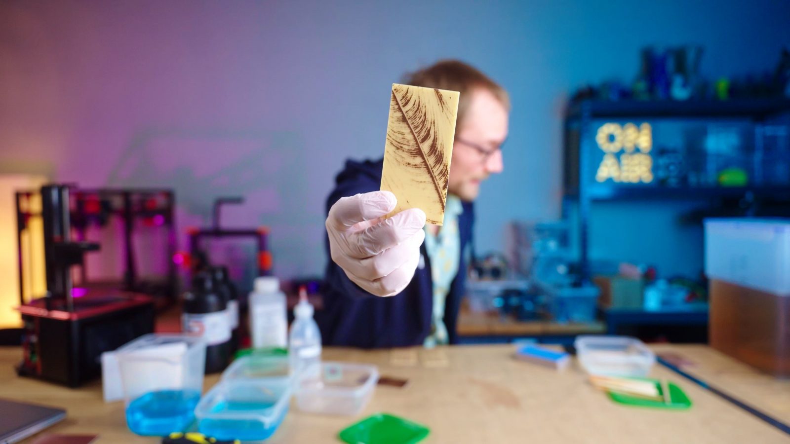
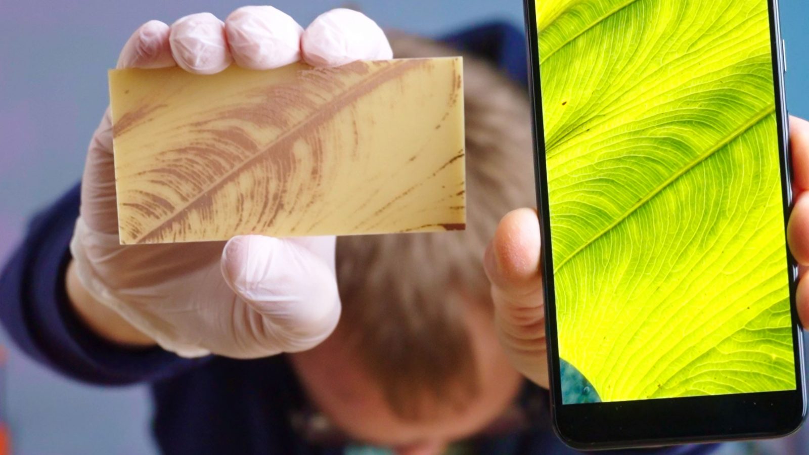
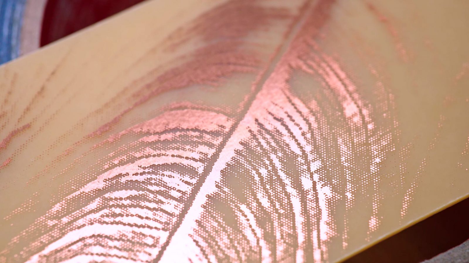
So one last cool thing that I did is to use the photoresist process for transferring an actual photo onto a PCB. You could do that just with black and white, but I first converted the photo to a half-tone image, then created an stl with a heightmap from it and used that to create a print file to expose the board. And it worked wonderfully! There’s lots of detail there, and if you want, you can still hot-air tin coat these for a bit more contrast.
So is this a practical process to etch your own PCBs? I think so, absolutely, yes. It’s definitely not going to replace ordering from a board house for larger orders, but when you need something right then and there or just want to cut out a bit of time from an iterating process, the 15 minutes of your time you have to spend to get a board etched can definitely be worth it. Sure, the process of getting the files out of Eagle and into the printer could be easier – and maybe there is an easier way with open-source software and hardware, but in either case, the results are really good!
I hope you found these experiments helpful or at least interesting – if you did, make sure to give the video a thumbs up and maybe even subscribe for more. Also, big shoutout to my Patrons and YouTube members, who help make this entire thing possible for me. Thank you.
And a thank you to everyone for watching, keep on making and happy holidays. See you!
Products shown in the video:
💙 Enjoying the videos? Support my work on Patreon!
Product links are affiliate links – I may earn a commission on qualifying purchases (at no extra cost to you)
Check out my second channel “More Layers” on YouTube for livestreams